PRODUCTS
Unveiling the PCB Mystery: A Comprehensive Guide from Basics to Applications
2025-04-20

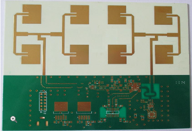
PCB (Printed Circuit Board), the "nervous system" of electronic devices, interconnects components through conductive traces on insulating substrates. Its evolution spans from single-sided boards to 60+ layer HDI (High-Density Interconnect) boards, with minimum line width 20μm. Modern PCBs adopt laser drilling technology, achieving ±0.05mm hole accuracy to meet the Df<0.002 ultra-low loss requirements for 5G base station PA modules. In AI servers, BMI (Bismaleimide) resin substrates with 220℃ temperature resistance and 10GHz ±3% impedance control become core materials for GB200/GB300 servers.
SUBSCRIBE
INQUIRY

